Janakpuri, Delhi
- GST NO. : 24AACCC7566J1ZG
PCB Assembly
Affordable & Quality PCB Assembling services for our customers
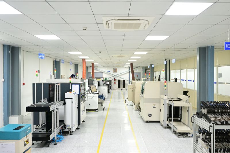
At C I Network Technologies, we are capable of supporting our customers in development of products. Quick turn PCB assembly shortens the product development cycle and requires efficiency and precision. With an attention to detail and precise execution, we offers end-to-end assembly services from prototype board design and assembly to high-volume printed circuit board assembly.
With a broad range of manufacturing capabilities from simple single-sided assemblies to complex densely populated fine pitch and BGA surface mount assemblies, our manufacturing lines are designed to achieve maximum performance in various application and technology sectors.
Our Electronics capabilities include:
Expertise in single, multi-layer flexible and rigid circuitry boards
Thorough design review prior to starting the assembly
Consignment or full turnkey solution
In-depth knowledge of various application requirements
Proficient in surface mounting, through-hole and mixed technology
Prompt response to design changes, requirement updates and questions
State-of-the-art advanced manufacturing equipment
Stringent quality inspections
Full compliance to RoHS standards
Reliable, repeatable precision services maximizing quality and reducing cost
List of our most popular PCB Assembly Services
Complete Printed Circuit Board Assembly
Rapid – Prototyping
New Product Introduction
Box Assembly & Integration
PCB Design & Engineering
PCB Fabrication
Quality Test & Burn-In
Failure Analysis
Mechanical Design & Engineering
LOADER:
- A PCB (Printed Circuit Board) loader is a device used to automate the process of loading PCB’s onto a production line. It is designed to efficiently handle and transport PCB’s from one stage of the manufacturing process to another.
- The main purpose of a PCB loader is to increase the productivity and efficiency of PCB assembly. It typically consists of a conveyor system or a magazine that holds multiple PCBs. The loader uses a combination of mechanical arms, belts, and sensors to feed the PCBs onto the production line in a controlled manner.
PRINTER:
- A PCB stencil is used in the process of applying solder paste onto a printed circuit board (PCB) during surface mount technology (SMT) assembly. It is a thin sheet, typically made of stainless steel or polyester film, that has precise openings or cutouts corresponding to the solder pads on the PCB.
- The purpose of a PCB stencil is to ensure accurate and consistent application of solder paste onto the solder pads of the PCB before components are placed. The stencil acts as a guide for depositing the solder paste in the right locations and in the right amounts.
3D SPI:
- Measurement Capabilities: Insufficient Paste, Excessive Paste, Missing-Paste, Bridging, Shape Deformity, Paste Displacement, Volume, Height, XY Position, Area
- Optical Measurement Unit: Vision Algorithm: 3D/PSMI (Phase Shifting Moire Interferometry)
- Software: 3D Inspection GUI, Gerber conversion software, SPC Plus software (Statistical Process Control) Operating System:Microsoft Windows 10
PICK & PLACE:
- Industry leader in loadable parts quantity with up to 130-part supple for any type of production with the flexibility to support part type changes.
- Flexibly supports high-speed placement of chip parts, as well as high-mix production using many large parts and odd-form parts.
- Supports various types of part supply packages from tape parts to tray and stick supplied parts, meeting the needs of high-mix production.
- High speed vision processing sustains placement quality without any drop in throughput.
- Faster part data creation, even for parts with unique shapes, further reducing the time required for adjustment.
REFLOW OVEN:
- A PCB reflow oven is a specialized equipment used to solder electronic components onto a printed circuit board (PCB). It employs controlled heating to melt the solder paste and create reliable connections between the components and the PCB.
COOLING CONVEYOR:
- A PCB cooling conveyor is a specialized equipment used in the electronics manufacturing industry to cool down printed circuit boards (PCBs) after the reflow soldering process. It provides a controlled environment to facilitate the cooling of PCBs and ensure the integrity of the solder joints.
- After the reflow soldering process in a reflow oven, where the solder paste has melted and formed reliable connections, the PCBs need to be gradually cooled to avoid thermal stress and maintain the integrity of the solder joints. A PCB cooling conveyor helps in achieving this cooling process efficiently and effectively.
3D Automated Optical Inspection:
- Measurement: Missing, Offset, Rotation, Polarity, Upside down, OCV, OCR, Coplanarity, Solder fillet, lifted lead, Lifted body, Billboarding, Tombstone, Bridging, Dimension etc.
- Optical Measurement Unit: 2D, 3D light projection unit
4 Way 3D projection Inspection Speed: 27cm2/sec
- Software: 4 Way 3D projection
UNLOADER:
- A PCB unloader is used to automate the process of removing printed circuit boards (PCBs) from a production line after assembly or inspection. It is designed to efficiently handle and transport PCBs from the end of the line to the next stage or for packaging. The main purpose of a PCB unloader is to increase the productivity and efficiency of the PCB assembly process by eliminating manual handling and streamlining the workflow. It typically consists of a conveyor system, mechanical arms, sensors, and other components to facilitate the smooth and controlled transfer of PCBs.
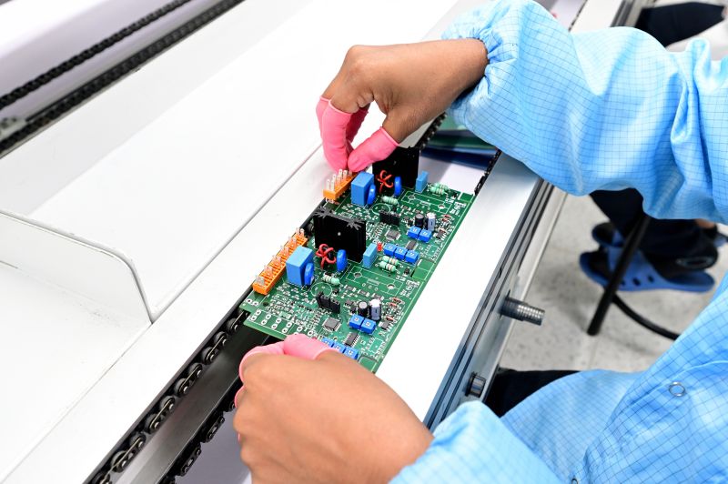
Through Hole Technology - Printed Circuit Board Assembly
Mixed Insertion
- Mixed insertion" is an assembly process in which different types of components are inserted into a printed circuit board (PCB). In mixed insertion, the PCB assembly may involve a combination of through-hole components and surface-mount components.
- Through-hole components have leads that are inserted into drilled holes on the PCB and soldered on the opposite side. Surface-mount components, on the other hand, are soldered directly onto the surface of the PCB without the need for holes.
WAVE SOLDERING
- Wave soldering is used to solder through-hole components onto printed circuit boards (PCBs). It is a highly efficient and reliable process that allows for the simultaneous soldering of multiple components.
LEAD CUTTING
- Wave soldering is used to solder through-hole components onto printed circuit boards (PCBs). It is a highly efficient and reliable process that allows for the simultaneous soldering of multiple components.
CLEANING
- Wave soldering is used to solder through-hole components onto printed circuit boards (PCBs). It is a highly efficient and reliable process that allows for the simultaneous soldering of multiple components.
TOUCHUP
- Wave soldering is used to solder through-hole components onto printed circuit boards (PCBs). It is a highly efficient and reliable process that allows for the simultaneous soldering of multiple components.


